The Nano SpotLight System is the latest addition to Kanomax FMT’s growing list of innovative technologies. Kanomax FMT partnered with Aerosol Devices and CT Associates to develop a new particle collection technique called Focused Aerosol Deposition or FAD.
While the semiconductor industry has been able to count nanometer sized particles for decades it has struggled to identify the elemental composition of the particles. When a “particle event” affecting semiconductor yield occurs in a semiconductor manufacturing facility, knowing the composition of the contaminating particles can be crucial in identifying the source of the event and eliminating the problem. Traditional Scanning Electron Microscopy (SEM) methods of attempting to collect these particles on a 25mm filter requires a long sample collection time (usually of several weeks). But in situations like this speed is essential to minimize manufacturing disruption. The Nano SpotLight’s System typical collection time is only 24 hours — a much better option for the industry than SEM.
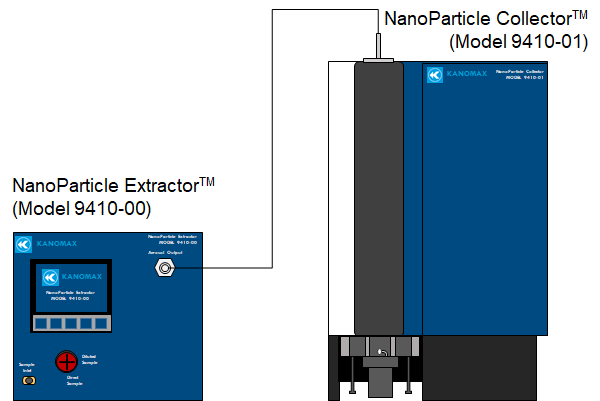
FAD uses a NanoParticle Nebulizer (NPN) to produce a droplet distribution of the suspect Ultrapure Water (UPW). Once each droplet is dried the resulting particles, formed from either real particles or non-volatile residue, are delivered to the Spot Sampler. The Spot Sampler uses a three-stage growth tube:
The substrate is either a 1 inch diameter silicon wafer or polycarbonate membrane mounted on a SEM stub. Once the collection surface is gold-coated the SEM technician can easily find the spot of particles in the exact center of the wafer and measure particle size as small as 5 nm. The technician can also perform Energy Dispersive Spectroscopy (EDS) analysis to identify the elemental composition of the particles.